| CPC H01L 21/76897 (2013.01) [H01L 21/283 (2013.01); H01L 21/28123 (2013.01); H01L 21/28229 (2013.01); H01L 21/28255 (2013.01); H01L 21/28562 (2013.01); H01L 21/31105 (2013.01); H01L 21/76802 (2013.01); H01L 21/76831 (2013.01); H01L 21/76849 (2013.01); H01L 21/76877 (2013.01); H01L 23/528 (2013.01); H01L 23/5226 (2013.01); H01L 23/535 (2013.01); H01L 29/0847 (2013.01); H01L 29/16 (2013.01); H01L 29/42364 (2013.01); H01L 29/456 (2013.01); H01L 29/4966 (2013.01); H01L 29/512 (2013.01); H01L 29/517 (2013.01); H01L 29/518 (2013.01); H01L 29/665 (2013.01); H01L 29/6656 (2013.01); H01L 29/66477 (2013.01); H01L 29/66545 (2013.01); H01L 29/78 (2013.01); H01L 29/785 (2013.01); H01L 29/495 (2013.01); H01L 2029/7858 (2013.01); H01L 2924/0002 (2013.01)] | 20 Claims |
|
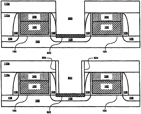
1. An integrated circuit structure, comprising:
a substrate comprising silicon;
a first structure above the substrate, the first structure comprising a first gate dielectric and a first gate electrode;
a first spacer adjacent to a first side of the first structure;
a second spacer adjacent to a second side of the first structure;
a second structure above the substrate, the second structure comprising a second gate dielectric and a second gate electrode;
a third spacer adjacent to a first side of the second structure;
a fourth spacer adjacent to a second side of the second structure;
a source or drain region between the second spacer and the third spacer;
a trench contact on the source or drain region;
a first inter-layer dielectric (ILD) layer directly on and vertically over the first spacer, the first structure, the second spacer, the third spacer, the second structure, and the fourth spacer, wherein the first ILD layer has a first opening vertically over the source or drain region, and wherein the first ILD layer is a planar ILD layer; and
a second ILD layer on the first ILD layer, wherein the second ILD layer has a second opening vertically over the first opening.
|