| CPC H01L 21/76801 (2013.01) [H01L 21/76822 (2013.01); H01L 21/76826 (2013.01); H01L 21/76829 (2013.01); H01L 21/76832 (2013.01); H01L 23/528 (2013.01); H01L 23/535 (2013.01); H01L 24/08 (2013.01); H01L 24/80 (2013.01); H04B 1/40 (2013.01); H01L 2224/08146 (2013.01); H01L 2224/80895 (2013.01)] | 18 Claims |
|
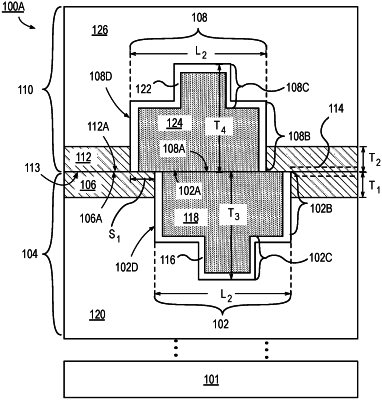
1. An integrated circuit (IC) interconnect structure, comprising:
a first dielectric material layer adjacent to at least a portion of a first interconnect feature;
a second interconnect feature in contact with at least a portion of the first interconnect feature;
a second dielectric material layer adjacent to at least a portion of the second interconnect feature;
a third dielectric material layer between the first and second dielectric material layers, wherein the third dielectric material layer is adjacent to the first interconnect feature and in contact with a portion of the second interconnect feature, and wherein the third dielectric material layer has a greater nitrogen content than at least the first dielectric material layer and wherein the third dielectric material layer comprises carbon; and
a fourth dielectric material layer between the second and third dielectric material layers, wherein the fourth dielectric material layer is adjacent to the second interconnect feature and in contact with a portion of the first interconnect feature, wherein the fourth dielectric material layer has a greater nitrogen content than at least the second dielectric material layer, and wherein the fourth dielectric material layer comprises carbon, and wherein carbon content within the third dielectric material layer decreases with proximity to the fourth dielectric material layer and wherein carbon content within the fourth dielectric material layer decreases with proximity to the third dielectric material layer.
|