| CPC H01L 21/6833 (2013.01) [H01J 37/32091 (2013.01); H01L 21/3065 (2013.01); H01L 21/67098 (2013.01); H01L 21/76826 (2013.01); H02N 13/00 (2013.01)] | 10 Claims |
|
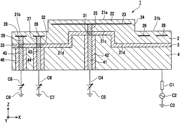
1. An electrostatic chuck device comprising:
an electrostatic chuck part having a sample placing surface on which a sample is placed and having a first electrode for electrostatic attraction;
a cooling base part placed on a side opposite to the sample placing surface with respect to the electrostatic chuck part to cool the electrostatic chuck part; and
an adhesive layer that bonds the electrostatic chuck part and the cooling base part together,
wherein the electrostatic chuck part has a recess on the adhesive layer side,
the cooling base part has a protrusion on the adhesion layer side,
a sheet resistance value of the first electrode is higher than 1.0Ω/□ and lower than 1.0×10¹⁰Ω/□, and
the adhesion layer is provided along the recess and protrusion.
|