| CPC H01L 21/56 (2013.01) [H01L 21/4839 (2013.01); H01L 21/78 (2013.01); H01L 23/544 (2013.01); H01L 2021/60007 (2013.01)] | 21 Claims |
|
1. A method of forming an electronic device, the method comprising:
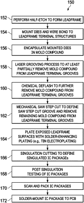
forming or accessing an encapsulated integrated circuit (IC) structure including a first die mounted on a first die attach pad of a leadframe, a second die mounted on a second die attach pad of the leadframe, a row of leadframe terminal structures of the leadframe between the first and second die attach pads, a leadframe terminal groove extending along the row of leadframe terminal structures, the leadframe terminal groove extending partially through a thickness of the row of leadframe terminal structures to define a reduced-thickness portion of the leadframe, and a mold compound encapsulating the first and second dies and at least partially filling the leadframe terminal groove;
after forming or accessing the encapsulated IC structure including the row of leadframe terminal structures and the leadframe terminal groove, performing a laser grooving process to remove a first amount of the mold compound from the leadframe terminal groove, wherein a remaining region of the mold compound remains in the leadframe terminal groove after the laser grooving process;
performing a saw step cut along the leadframe terminal groove extending through a partial depth of respective ones of the row of leadframe terminal structures to define a saw step cut groove, the saw step cut groove having a lateral width larger than a lateral width of the leadframe terminal groove, the saw step cut removing the remaining region of mold compound from the leadframe terminal groove;
performing a plating process to plate exposed surfaces of respective ones of the row of leadframe terminal structures, including exposed surfaces of the saw step cut groove, with a solder-enhancing plating material; and
performing a singulation process to define a first IC package including the first die and a second IC package including the second die, the singulation process including a singulation cut extending along the row of leadframe terminal structures and aligned with the saw step cut groove, the singulation cut dividing respective ones of the row of leadframe terminal structures into (a) a first leadframe terminal of the first IC package, the first leadframe terminal having a first terminal end surface and (b) a second leadframe terminal of the second IC package, the second leadframe terminal having a second terminal end surface;
wherein the singulation cut has a lateral width smaller than the lateral width of the saw step cut groove such that a region of solder-enhancing plating material remains on the first terminal end surface and second terminal end surface defined by the singulation cut.
|