| CPC H01L 21/3086 (2013.01) [H10B 12/053 (2023.02); H10B 12/34 (2023.02)] | 18 Claims |

|
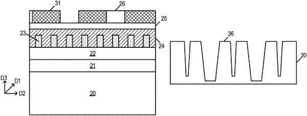
1. A method for forming an active region array, comprising the following steps:
providing a substrate;
forming a first mask layer on a surface of the substrate, a first etched pattern being provided in the first mask layer;
forming a second mask layer covering a surface of the first mask layer;
forming a third mask layer having a second etched pattern on a surface of the second mask layer;
forming a flank covering a sidewall of the second etched pattern;
removing the third mask layer to form a third etched pattern between adjacent flanks;
etching the first mask layer along the third etched pattern to form a fourth etched pattern in the first mask layer; and
etching the substrate along the first etched pattern and the fourth etched pattern, to form multiple active regions in the substrate.
|