| CPC H01L 21/26586 (2013.01) [H01L 29/0847 (2013.01); H01L 29/6659 (2013.01); H01L 29/7833 (2013.01)] | 14 Claims |
|
1. A method of manufacturing a semiconductor device, comprising:
forming a doped region having a first conductive type, and forming a gate structure on the doped region;
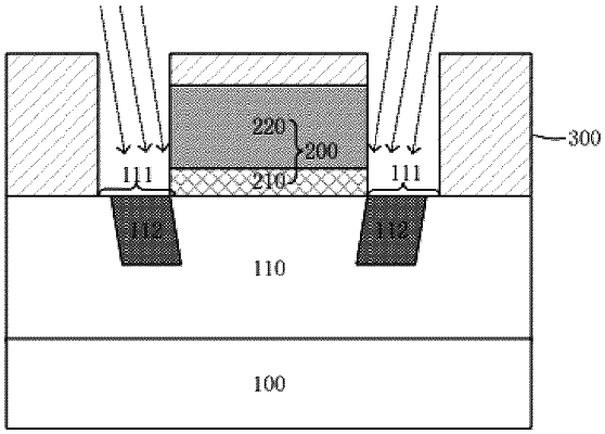
implanting doping ions having the first conductive type to a first region of the doped region along a tilt direction inclining toward the gate structure, and then annealing, so as to form a Halo region; and
implanting doping ions having a second conductive type to a second region of the doped region along a vertical direction, so as to form a source/drain region having the second conductive type;
wherein the step of implanting the doping ions and then annealing, so as to form a Halo region, comprises:
forming a mask on the doped region, the first region of the doped region being defined and exposed by the mask;
implanting the doping ions to the exposed first region along the tilt direction inclining toward the gate structure, so as to form a dopant implanted region extending obliquely in the doped region; and
annealing, so that the dopant implanted region diffuses to surroundings so as to form the Halo region;
wherein the first region is adjacent to the gate structure and the second region is located on the side of the first region facing away from the gate structure, and the first region and the second region have no overlap region, and
wherein the Halo region is located on the side of the source/drain region facing the gate structure and extends to the gate structure from a side surface of the source/drain region and contacts a bottom surface of the gate structure.
|