| CPC H01L 21/0337 (2013.01) [H01L 21/31144 (2013.01); H01L 21/76802 (2013.01); H01L 21/76877 (2013.01)] | 20 Claims |

|
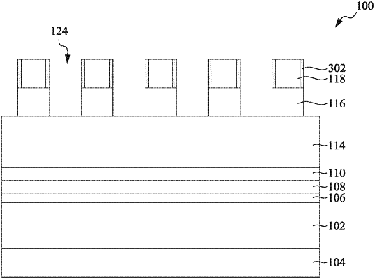
1. A method of forming a semiconductor device, the method comprising:
patterning a photoresist layer on a mask layer;
performing an oxygen plasma treatment on the photoresist layer, the oxygen plasma treatment converting the photoresist layer to a treated photoresist layer by oxidizing an exposed surface of the photoresist layer;
after the performing the oxygen plasma treatment patterning the mask layer using the treated photoresist layer as a mask, wherein during an etching of the mask layer the treated photoresist layer is an oxidized organic material; and
patterning a target layer using the patterned mask layer as a mask.
|
|
8. A method of forming a semiconductor device, the method comprising:
forming a film over a patterned top layer, the patterned top layer being on a mask layer, the mask layer being over a target layer, wherein openings extend through the patterned top layer to expose the mask layer, a first portion of the film over the patterned top layer has a first thickness, a second portion of the film on a bottom surface of the openings has a second thickness, and the first thickness is greater than the second thickness;
patterning the mask layer using the patterned top layer as a mask; and
using the patterned mask layer as a mask to pattern the target layer.
|
|
15. A method of forming a semiconductor device, the method comprising:
forming a film stack over a target layer, the target layer being on a substrate;
forming a photoresist over the film stack, the photoresist comprising a bottom layer, a middle layer over the bottom layer, and a top layer over the middle layer;
patterning the top layer, wherein the patterning the top layer forms first openings through the patterned top layer;
forming an oxide layer on exposed surfaces of the patterned top layer and over bottom surfaces of the first openings, wherein the oxide layer has a first thickness on the exposed surfaces of the patterned top layer and a second thickness over the bottom surfaces of the first openings, wherein the first thickness is greater than the second thickness;
patterning the middle layer using the patterned top layer as a mask;
patterning the bottom layer using the patterned middle layer as a mask;
patterning the film stack using the patterned bottom layer as a mask;
patterning the target layer using the patterned film stack as a mask to form second openings through the target layer; and
forming conductive features in the second openings.
|