US 11,887,845 B2
Method for producing three-dimensional structure, method for producing vertical transistor, vertical transistor wafer, and vertical transistor substrate
Kazutaka Kamijo, Kitakanbara-gun (JP); Etsuo Fukuda, Kitakanbara-gun (JP); Takashi Ishikawa, Kitakanbara-gun (JP); Koji Izunome, Kitakanbara-gun (JP); Moriya Miyashita, Kitakanbara-gun (JP); Takao Sakamoto, Kitakanbara-gun (JP); and Tetsuo Endoh, Sendai (JP)
Assigned to GLOBALWAFERS JAPAN CO., LTD., Niigata (JP); and TOHOKU UNIVERSITY, Sendai (JP)
Filed by GLOBALWAFERS JAPAN CO., LTD., Niigata (JP); and TOHOKU UNIVERSITY, Sendai (JP)
Filed on Sep. 29, 2021, as Appl. No. 17/488,883.
Application 17/488,883 is a division of application No. 16/632,607, previously published as PCT/JP2018/026702, filed on Jul. 17, 2018.
Claims priority of application No. 2017-140079 (JP), filed on Jul. 19, 2017.
Prior Publication US 2022/0093396 A1, Mar. 24, 2022
Int. Cl. H01L 21/02 (2006.01); H01L 29/66 (2006.01)
CPC H01L 21/02255 (2013.01) [H01L 21/02238 (2013.01); H01L 29/66666 (2013.01)] 5 Claims
OG exemplary drawing
 
1. A method for producing a three-dimensional structure, comprising:
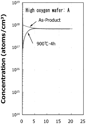
processing a surface layer of a silicon substrate to form a three-dimensional shape, the surface layer having an oxygen concentration of 1×10¹⁸ atoms/cm3 or ore; and
performing a heat treatment to form an oxide film on a surface of the three-dimensional shape to produce the three-dimensional structure, the three-dimensional structure having an oxygen concentration of 1×10¹⁷ atoms/cm3 or more and projections and recesses in a thickness direction of the silicon substrate, a height of the three-dimensional structure in the thickness direction being between 1 nm and 100 nm, wherein
the heat treatment temperature is in a range of 800° C. to 900° C.