| CPC H01L 24/13 (2013.01) [H01L 24/02 (2013.01); H01L 2224/0239 (2013.01); H01L 2224/02311 (2013.01); H01L 2224/02381 (2013.01); H01L 2224/13111 (2013.01); H01L 2224/13124 (2013.01); H01L 2224/13139 (2013.01); H01L 2224/13144 (2013.01); H01L 2224/13147 (2013.01); H01L 2224/13155 (2013.01); H01L 2224/13166 (2013.01); H01L 2224/13171 (2013.01); H01L 2224/13172 (2013.01); H01L 2224/13184 (2013.01)] | 20 Claims |
|
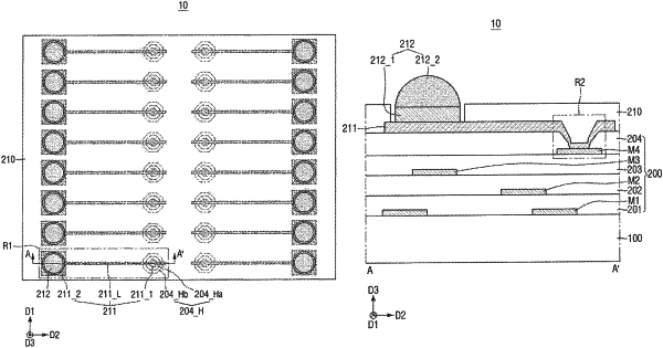
1. A semiconductor device comprising:
a substrate;
a conductive layer disposed on the substrate and extending in a first direction;
an insulating layer disposed on the conductive layer and exposing at least a portion of the conductive layer through a via hole defined therein, wherein the via hole includes:
a first face extending in a first slope relative to a top face of the conductive layer; and
a second face extending in a second slope relative to the top face of the conductive layer, the second slope is less than the first slope; and
a redistribution conductive layer including:
a first pad area disposed in the via hole; and
a line area at least partially extending along the first face and the second face,
wherein the first face directly contacts the conductive layer, and the second face is positioned at a level higher than a level of the first face in a second direction perpendicular to a top face of the substrate.
|