| CPC H01J 37/32697 (2013.01) [H01J 37/32027 (2013.01); H05H 1/54 (2013.01)] | 21 Claims |
|
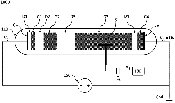
1. A method for processing a surface of a substrate, the method comprising:
placing a substrate on a support stage in a region of a DC plasma reaction chamber configured to produce a positive column of DC plasma;
generating the DC plasma;
presetting a potential at the surface of the substrate to a reference potential; and
capacitively coupling, to the support stage, a periodic biasing signal having a biasing voltage that is referenced to the reference potential, the periodic biasing signal comprising:
an active phase having a positive voltage that is based on a known reaction threshold voltage of targeted chemical bonds of atoms at the surface of a substrate;
a neutralization phase having a negative voltage; and
an initialization phase having a zero voltage.
|