| CPC H01J 1/312 (2013.01) [C23C 16/342 (2013.01); H01J 1/90 (2013.01); H01J 9/027 (2013.01); H01J 2209/012 (2013.01)] | 15 Claims |
|
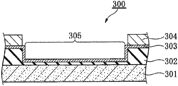
1. An electron emitting element comprising:
a laminated structure in which a first electrode, an electron accelerating layer made of an insulation film, a second electrode, and a cover film are laminated in that order, wherein
the second electrode is an electrode which transmits electrons and emits electrons from a surface thereof, and
the cover film is a film which transmits electrons, is a protective film made of a material different from that of the second electrode, and constitutes an electron emission surface thereof,
wherein the cover film is made of hexagonal boron nitride.
|