| CPC G11C 7/222 (2013.01) [G11C 7/1009 (2013.01); G11C 7/109 (2013.01); G11C 7/1063 (2013.01); G11C 8/18 (2013.01)] | 10 Claims |

|
1. An operation method of a memory module which includes a plurality of memory devices, the method comprising:
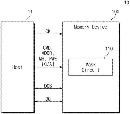
receiving a partial write command including a partial write enable signal and a plurality of mask signals, at a first time;
during a strobe toggle interval after the first time, receiving a first data strobe signal toggling through a first data strobe line connected with a first memory device, among the plurality of memory devices, and receiving a second data strobe signal maintained at logic high through a second data strobe line connected with a second memory device, among the plurality of memory devices; and
receiving a plurality of data through a plurality of data lines, during a data input interval after the first time.
|