| CPC G11C 7/12 (2013.01) [G11C 7/1039 (2013.01); G11C 7/18 (2013.01)] | 25 Claims |
|
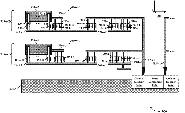
1. An apparatus, comprising:
a first digit line associated with a first level of a memory die above a substrate, the first digit line coupled with a first set of memory cells of the memory die;
a second digit line associated with a second level of the memory die above the substrate, the second digit line coupled with a second set of memory cells of the memory die;
a first transistor associated with the first level of the memory die and operable to couple the first digit line with a first conductor that is coupled with a sense amplifier of the memory die;
a second transistor associated with the second level of the memory die and operable to couple the second digit line with the first conductor;
a third transistor associated with the first level of the memory die and operable to couple the first conductor with a voltage source; and
a fourth transistor associated with the second level of the memory die and having a channel portion coupled between the first conductor and a second conductor.
|