| CPC G11C 7/1039 (2013.01) [G11C 7/109 (2013.01); G11C 7/1012 (2013.01); G11C 7/1063 (2013.01); G11C 7/1066 (2013.01); G11C 7/1093 (2013.01)] | 24 Claims |
|
1. A memory device, comprising:
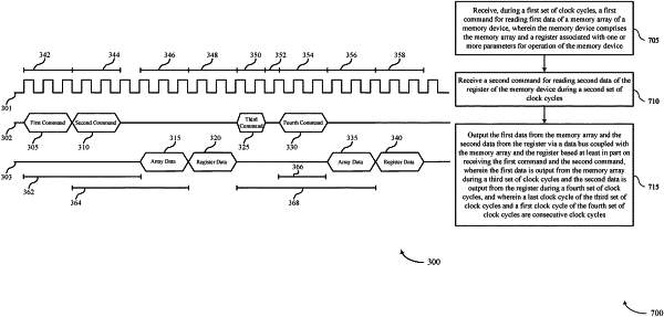
a memory array comprising a plurality of memory cells configured to store first data, wherein the first data is output from the memory array based at least in part on the memory device receiving a first command;
a first buffer coupled with the memory array and configured to buffer the first data based at least in part on the first data being output from the memory array;
a register configured to store second data, wherein the second data is output from the register based at least in part on the memory device receiving a second command different than the first command;
a second buffer coupled with the register and configured to buffer the second data based at least in part on the second data being output from the register; and
a multiplexer coupled with the first buffer, the second buffer, and a data bus, wherein the multiplexer is configured to output the first data and the second data on the data bus during consecutive sets of clock cycles, wherein a first latency between the memory device receiving the first command and the multiplexer outputting the first data is the same as a second latency between the memory device receiving the second command and the multiplexer outputting the second data.
|