| CPC G11C 17/06 (2013.01) [G11C 17/18 (2013.01)] | 15 Claims |

|
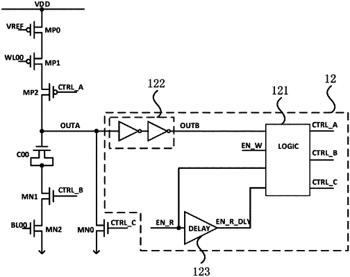
1. An anti-fuse memory cell circuit, comprising:
an anti-fuse device;
a switch module, coupled to the anti-fuse device;
a selection module, coupled to the switch module; and
a control module, respectively coupled to the anti-fuse device and the switch module;
wherein, the control module is configured to switch an on-off mode of the switch module according to a breakdown state of the anti-fuse device;
wherein the anti-fuse device has a first end and a second end,
wherein the switch module includes a first switch unit and a second switch unit, wherein each of the first switch unit and the second switch unit has a first terminal, a second terminal and a control terminal, wherein the control terminal is coupled to the control module; and
wherein the second terminals of the first and the second switch units are each coupled to the selection module, wherein the first terminal of the first switch unit is coupled to the first end of the anti-fuse device, and wherein the first terminal of the second switch unit is coupled to the second end of the anti-fuse device.
|