| CPC G11C 16/3459 (2013.01) [G11C 16/0483 (2013.01); G11C 16/10 (2013.01); H10B 41/27 (2023.02); H10B 43/27 (2023.02)] | 20 Claims |
|
1. A method of programming a memory device, comprising the steps of:
preparing a memory device that includes an array of memory cells arranged in a plurality of word lines;
programming the memory cells of a selected word line of the plurality of word lines in a plurality of program-verify iterations;
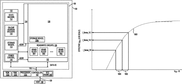
during a verify portion of at least one program-verify iteration of the plurality of program-verify iterations, determining a threshold voltage of at least one memory cell of the selected word line relative to a first verify low voltage VL1, a second verify low voltage VL2, and a verify high voltage VH associated with a data state being programmed; and
wherein the step of determining the threshold voltage of the at least one memory cell includes maintaining a count of program-verify iterations since the at least one memory cell passed a verify high voltage of a previously programmed data state or includes discharging a sense node through a channel including the at least one memory cell and comparing a discharge time to predetermined sense times associated with the first and second verify low voltages and with the verify high voltage.
|