| CPC G11C 16/10 (2013.01) [G11C 16/0483 (2013.01); G11C 16/08 (2013.01); G11C 16/24 (2013.01); G11C 16/26 (2013.01); G11C 16/3459 (2013.01)] | 20 Claims |
|
1. A memory device comprising:
a memory array comprising a plurality of memory cells configured as a multi-level cell (MLC) memory; and
control logic, operatively coupled with the memory array, to perform operations comprising:
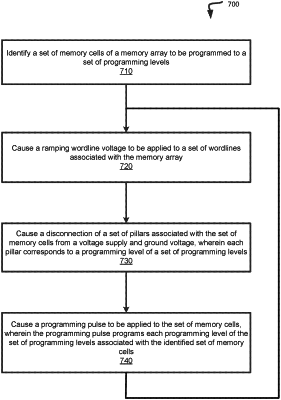
identifying a set of memory cells to be programmed during a program operation;
causing, during a first time period of the program operation, a ramping wordline voltage to be applied to a set of wordlines associated with the memory array;
causing, during the first time period, a disconnection of a set of pillars associated with the set of memory cells from a voltage supply and ground voltage, wherein each pillar corresponds to a respective programming level of a set of programming levels; and
causing, during a second time period of the program operation, a programming pulse to be applied to the set of memory cells, wherein the programming pulse programs each programming level of the set of programming levels associated with the identified set of memory cells.
|