| CPC G11C 16/0483 (2013.01) [H01L 29/66795 (2013.01); H01L 29/7851 (2013.01); H10B 41/10 (2023.02); H10B 41/27 (2023.02); H10B 41/35 (2023.02); H10B 43/10 (2023.02); H10B 43/27 (2023.02); H10B 43/35 (2023.02)] | 21 Claims |

|
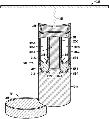
1. A memory device comprising:
a vertical pillar of memory cells;
a data line;
a transistor to couple the data line to the vertical pillar of memory cells, the transistor having a channel structure and a gate, the channel structure separated from the gate;
a first portion of the channel structure of the transistor coupled to channel material of the vertical pillar of memory cells and extending vertically from the channel material; and
a segmented portion of the channel structure extending vertically from the first portion, the segmented portion having a fin contacting and extending vertically from the first portion of the channel structure and a non-conductive region contacting and extending vertically from the first portion of the channel structure, the first portion having a border with the non-conductive region, with the border decreasing from the fin to a location below a lowest level of the fin.
|
|
6. A memory device comprising:
a vertical pillar of memory cells;
a data line;
a transistor to couple the data line to the vertical pillar of memory cells, the transistor having a channel structure and a gate, the channel structure separated from the gate;
a first portion of the channel structure of the transistor coupled to channel material of the vertical pillar of memory cells and extending vertically from the channel material;
a segmented portion of the channel structure extending vertically from the first portion, the segmented portion having a fin contacting and extending vertically from the first portion of the channel structure and a non-conductive region contacting and extending vertically from the first portion of the channel structure; and
a fanged region extending from the fin into the first portion of the channel structure.
|
|
15. A memory system comprising:
multiple memory devices, with one or more of the memory devices including:
data lines;
a memory array having vertical strings of memory cells with each vertical string arranged as a pillar coupled to a transistor, the transistor coupling the string to
a data line of the data lines, the transistor having:
a channel structure and a gate, the channel structure separated from the gate;
a first portion of the channel structure coupled to channel material of the vertical string and extending vertically from the channel material; and
a segmented portion of the channel structure extending vertically from the first portion, the segmented portion having a fin contacting and extending vertically from the first portion of the channel structure and a non-conductive region contacting and extending vertically from the first portion of the channel structure; and
a fanged region extending from the fin into the first portion of the channel structure; and
a memory controller including processing circuitry, the memory controller configured to perform operations including performance of an erase operation on a selected string of the memory array with application of an erase voltage to the gate of the transistor coupling the selected string to the data line associated with the selected string.
|