| CPC G11C 13/003 (2013.01) [G11C 13/0004 (2013.01); G11C 13/004 (2013.01); G11C 13/0023 (2013.01); G11C 13/0069 (2013.01); G11C 2213/71 (2013.01)] | 25 Claims |
|
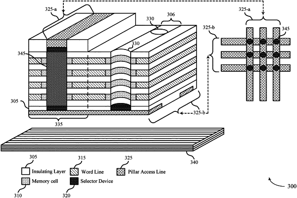
1. An apparatus, comprising:
a plurality of first layers each comprising a respective memory material element coupled with a respective first electrode;
a pillar extending through the plurality of first layers and coupled with each of the respective memory material elements, wherein a memory material element of the respective memory material elements is operable to be accessed based at least in part on a voltage difference between the pillar and a first electrode coupled with the memory material element;
a first selector device coupled with a first portion of the pillar that is above the plurality of first layers;
a second selector device coupled with a second portion of the pillar that is below the plurality of first layers;
a second electrode coupled with the first selector device and operable to apply a first selection voltage to the first selector device; and
a third electrode coupled with the second selector device and operable to apply a second selection voltage to the second selector device.
|