| CPC G11C 11/4091 (2013.01) [G11C 7/04 (2013.01)] | 15 Claims |

|
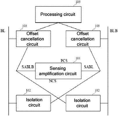
1. An amplifier circuit, coupled to a bit line and a complementary bit line, and comprising:
a sensing amplification circuit, comprising a readout node, a complementary readout node, a first node, and a second node, wherein at a sensing amplification stage and an offset cancellation stage, the first node is configured to receive a high level, and the second node is configured to receive a low level;
an isolation circuit, coupled to the readout node, the complementary readout node, the bit line, and the complementary bit line, wherein the isolation circuit is configured to couple the readout node to the bit line and the complementary readout node to the complementary bit line at the sensing amplification stage;
an offset cancellation circuit, coupled to the bit line, the complementary bit line, the readout node, and the complementary readout node, wherein the offset cancellation circuit is configured to couple the bit line to the complementary readout node and the complementary bit line to the readout node at the offset cancellation stage; and
a processing circuit, coupled to the offset cancellation circuit, and configured to obtain a memory temperature and adjust duration of the offset cancellation stage based on the memory temperature.
|