| CPC G11C 11/4091 (2013.01) [G11C 11/4094 (2013.01); G11C 11/4096 (2013.01)] | 20 Claims |

|
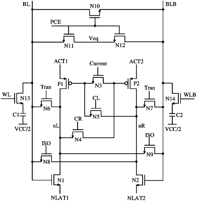
1. A sense amplifier, comprising:
an amplification circuit arranged to read a data in a memory cell on a first bit line or a second bit line; and
a control circuit, electrically connected to the amplification circuit;
wherein in a case of reading the data in the memory cell on the first bit line, at an offset compensation stage of the sense amplifier, the control circuit is arranged to configure the amplification circuit to comprise a first diode structure, a first current mirror structure, and a first inverter with an input terminal and an output terminal connected to each other;
in a case of reading the data in the memory cell on the second bit line, at the offset compensation stage of the sense amplifier, the control circuit is arranged to configure the amplification circuit to comprise a second diode structure, a second current mirror structure, and a second inverter with an input terminal and an output terminal connected to each other.
|