| CPC G11C 11/4085 (2013.01) [G11C 11/4087 (2013.01); H10B 12/315 (2023.02)] | 20 Claims |

|
1. A memory device comprising:
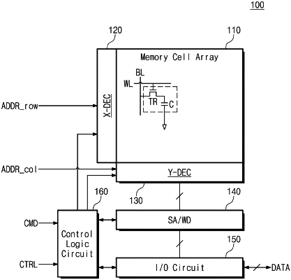
a row decoder configured to generate a plurality of word line control signals, based on a row address received from an external device;
a first sub-array including a plurality of memory cells connected with a plurality of word lines;
a first sub-word line driver configured to provide a selection voltage or a non-selection voltage to odd-numbered word lines of the plurality of word lines, based on odd-numbered word line control signals corresponding to the odd-numbered word lines; and
a second sub-word line driver configured to provide the selection voltage or the non-selection voltage to even-numbered word lines of the plurality of word lines, based on even-numbered word line control signals corresponding to the even-numbered word lines,
wherein the first sub-word line driver is further configured to apply the non-selection voltage to non-selection word lines of the even-numbered word lines, in response to the even-numbered word line control signals, and
wherein the second sub-word line driver is further configured to apply the non-selection voltage to non-selection word lines of the odd-numbered word lines, in response to the odd-numbered word line control signals.
|