| CPC G11C 11/24 (2013.01) [G11C 11/404 (2013.01); H01L 28/40 (2013.01); H10B 12/395 (2023.02)] | 20 Claims |

|
13. A method for manufacturing an integrated circuit chip, comprising:
forming a doped region in a substrate from a first main surface, the substrate having an opposing second main surface;
forming a transistor at a first location of the first main surface of the substrate; and
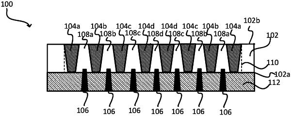
forming a capacitor at a second location of the substrate, the capacitor comprising:
a first conductive line and a second conductive line that are formed from the doped region of the substrate and extends from the first main surface to the second main surface of the substrate;
an insulating structure that is formed between the first and second conductive lines and extends from the first main surface to the second main surface; and
contacts formed in a dielectric layer and arranged along the first and second conductive lines, the dielectric layer being formed over the first main surface of the substrate, the contacts extending through the dielectric layer and into the first and second conductive lines.
|