| CPC G11C 11/161 (2013.01) [H10B 61/00 (2023.02); H10N 50/01 (2023.02); H10N 50/10 (2023.02); H10N 50/80 (2023.02); H10N 50/85 (2023.02); G11C 11/16 (2013.01)] | 20 Claims |
|
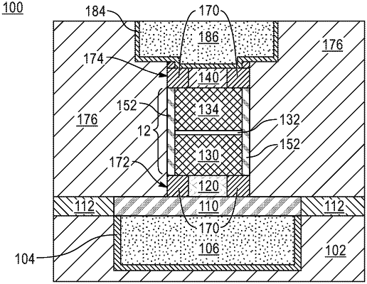
1. A memory device, comprising:
a magnetic tunnel junction pillar surrounded by sidewall spacers, the magnetic tunnel junction pillar being located between a top electrode and a bottom electrode;
an amorphous dielectric hardmask in contact with a first portion of an uppermost surface of the magnetic tunnel junction pillar;
a first portion of a metal layer disposed on opposite sidewalls of the amorphous dielectric hardmask, the first portion of the metal layer being in contact with a second portion of the uppermost surface of the magnetic tunnel junction pillar extending outwards from the amorphous dielectric hardmask and an uppermost surface of the sidewall spacers, the first portion of the metal layer providing the top electrode;
a dielectric underlayer in contact with a first portion of a bottommost surface of the magnetic tunnel junction pillar; and
a second portion of the metal layer disposed on opposite sidewalls of the dielectric underlayer, the second portion of the metal layer being in contact with a second portion of the bottommost surface of the magnetic tunnel junction pillar extending outwards from the dielectric underlayer and a bottommost surface of the sidewall spacers, the second portion of the metal layer providing the bottom electrode.
|