| CPC G09G 3/3677 (2013.01) [G02F 1/1345 (2013.01); G02F 1/1368 (2013.01); G11C 19/28 (2013.01); G11C 19/287 (2013.01); G02F 1/136286 (2013.01); G02F 1/136295 (2021.01); G02F 2201/56 (2013.01); G09G 2300/0426 (2013.01); G09G 2310/0286 (2013.01); G09G 2310/08 (2013.01)] | 12 Claims |

|
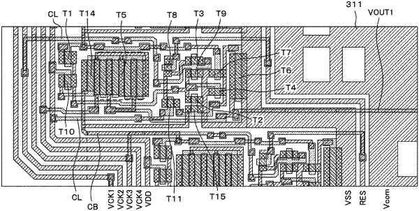
1. A display device comprising:
a substrate having a display region and a peripheral region;
a scanning line drive circuit having a first unit circuit and a second unit circuit at the peripheral region; and
a plurality of wirings provided outside and along the scanning line drive circuit in a plan view at the peripheral region,
wherein
the plurality of wirings include a plurality of clock wirings, a first power wiring and a second power wiring,
each of the first power wiring and the second power wiring is not supplied with a clock signal,
a layout of the first power wiring is provided the closest to the scanning line driver circuit among the plurality of wirings between an outer edge of the substrate and the scanning line drive circuit, in the plan view,
a layout of the plurality of clock wirings is provided between the first power wiring and the outer edge of the substrate,
a layout of the second power wiring is provided the closest to the scanning line driver circuit among the plurality of wirings between the scanning line drive circuit and the display region, in the plan view,
none of the plurality of clock wirings is provided between the first power wiring and the scanning line drive circuit, in the plan view,
the second unit circuit is shifted from the first unit circuit in a first direction, and is shifted from the first unit circuit in a second direction which crosses the first direction,
the first unit circuit and the second unit circuit are connected via a coupling wiring, and
a layout of the coupling wiring is provided between the first power wiring and the second power wiring, in the plan view.
|