| CPC G09G 3/3674 (2013.01) [G09G 3/3677 (2013.01); G11C 19/28 (2013.01); G09G 3/3266 (2013.01); G09G 2230/00 (2013.01); G09G 2300/0408 (2013.01); G09G 2300/0426 (2013.01); G09G 2310/0267 (2013.01); G09G 2310/0286 (2013.01); G09G 2320/0257 (2013.01); G11C 19/287 (2013.01)] | 14 Claims |
|
1. A drive method of a gate drive circuit, the gate drive circuit including at least two cascaded shift registers, each register including a pull-up node, a first pull-down node, an input sub-circuit, a first noise reduction sub-circuit and a first pull-down sub-circuit, the first noise reduction sub-circuit being coupled to the pull-up node, the first pull-down node and a first voltage signal terminal, the input sub-circuit being coupled to the pull-up node and a signal input terminal, the first pull-down sub-circuit being coupled to the signal input terminal, the first pull-down node and the first voltage signal terminal, the drive method comprising:
a noise reduction phase and a charging phase included in a frame period for each shift register in the gate drive circuit, wherein the noise reduction phase including:
transmitting, by the first noise reduction sub-circuit, a first voltage signal received at the first voltage signal terminal to the pull-up node after the first noise reduction sub-circuit is turned on under control of a voltage of the first pull-down node;
the charging phase including:
transmitting, by the input sub-circuit, an input signal received at the signal input terminal to the pull-up node after the input sub-circuit is turned on under control of the input signal transmitted by the signal input terminal;
transmitting, by the first pull-down sub-circuit, the first voltage signal received at the first voltage signal terminal to the first pull-down node after the first pull-down sub-circuit is turned on under the control of the input signal; and
stopping transmitting, by the first noise reduction sub-circuit, the first voltage signal received at the first voltage signal terminal to the pull-up node after the first noise reduction sub-circuit is turned off under the control of the voltage of the first voltage signal transmitted to the first pull-down node, wherein the method further comprises:
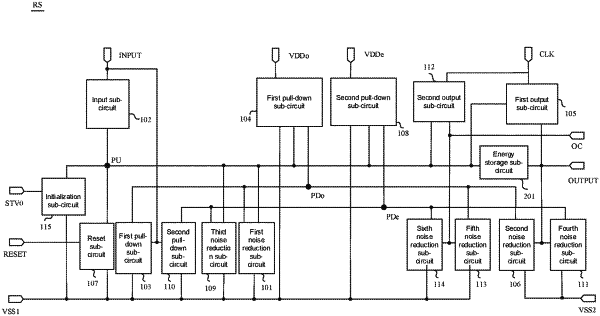
an operation of raising gate scanning signals output by all shift registers included in the gate drive circuit before a display apparatus to which the gate drive circuit is applied is shut down, wherein the shift register further includes a reset sub-circuit, an initialization sub-circuit, a first pull-down control sub-circuit, a first output sub-circuit, a second noise reduction sub-circuit, a second output sub-circuit and a fifth noise reduction sub-circuit the reset sub-circuit is coupled to the pull-up node, the first voltage signal terminal and a reset signal terminal;
the initialization sub-circuit is coupled to the pull-up node, an initialization signal terminal and the first voltage signal terminal;
the first pull-down control sub-circuit is coupled to the first voltage signal terminal, a second voltage signal terminal, the pull-up node and the first pull-down node;
the first output sub-circuit is coupled to a clock signal terminal, the pull-up node and a first signal output terminal;
the second noise reduction sub-circuit is coupled to the first pull-down node, a third voltage signal terminal and the first signal output terminal;
the second output sub-circuit is coupled to the pull-up node, the clock signal terminal and a second signal output terminal; and
the fifth noise reduction sub-circuit is coupled to the first pull-down node, the first voltage signal terminal and the second signal output terminal;
wherein a signal input terminal of a first-stage shift register is coupled to a start signal terminal;
a signal input terminal of an any-stage shift register except the first-stage shift register is coupled to a second signal output terminal of a previous-stage shift register of the any-stage shift register;
a reset signal terminal of an any-stage shift register except a last-stage shift register is coupled to a second signal output terminal of a next-stage shift register of the any-stage shift register;
a reset signal terminal of the last-stage shift register is coupled to a signal terminal separately provided for outputting a reset signal, or is coupled to the start signal terminal; and
a first signal output terminal of each shifter register is coupled to a single gate line;
wherein the operation of raising the gate scanning signals output by all shift registers included in the gate drive circuit, includes:
pulling down the first voltage signal output by the first voltage signal terminal and a start signal output by the start signal terminal to ground, and raising an initialization signal output by the initialization signal terminal, a second voltage signal output by the second voltage signal terminal, a third voltage signal output by the third voltage signal terminal and a clock signal output by the clock signal terminal, so that the initialization sub-circuit is turned on under control of the initialization signal, and the initialization sub-circuit transmits the first voltage signal to the pull-up node after, such that a voltage of the pull-up node is a grounding voltage;
the first pull-down control sub-circuit transmits the second voltage signal to the first pull-down node in response to the second voltage signal and the grounding voltage of the pull-up node, such that a voltage of the first pull-down node is raised;
the second noise reduction sub-circuit is turned on under control of the voltage of the first pull-down node, and the second noise reduction sub-circuit transmits the third voltage signal to the first signal output terminal, such that a voltage of a gate scanning signal output by the first signal output terminal is raised:
the first noise reduction sub-circuit is turned on under the control of the voltage of the first pull-down node, and the first noise reduction sub-circuit transmits the first voltage signal to the pull-up node, such that the voltage of the pull-up node is the grounding voltage; and
the fifth noise reduction sub-circuit is turned on under the control of the voltage of the first pull-down node, and the fifth noise reduction sub-circuit transmits the first voltage signal to the second signal output terminal, such that a voltage of a signal output by the second signal output terminal is the grounding voltage; or
wherein the operation of raising the gate scanning signals output by all shift registers included in the gate drive circuit, includes:
pulling down the first voltage signal output by the first voltage signal terminal, a start signal output by the start signal terminal and an initialization signal output by the initialization signal terminal to ground, and raising a second voltage signal output by the second voltage signal terminal, a third voltage signal output by the third voltage signal terminal and a clock signal output by the clock signal terminal, so that the initialization sub-circuit is turned off under control of the initialization signal, the first pull-down control sub-circuit transmits the second voltage signal to the first pull-down node in response to the second voltage signal and a voltage of the pull-up node, such that a voltage of the first pull-down node is raised;
the second noise reduction sub-circuit is turned on under control of the voltage of the first pull-down node, and the second noise reduction sub-circuit transmits the third voltage signal to a first signal output terminal, such that a voltage of a gate scanning signal output by the first signal output terminal is raised;
the first noise reduction sub-circuit is turned on under the control of the voltage of the first pull-down node, and the first noise reduction sub-circuit transmits the first voltage signal to the pull-up node, such that the voltage of the pull-up node is the grounding voltage; and
the fifth noise reduction sub-circuit is turned on under the control of the voltage of the first pull-down node, and the fifth noise reduction sub-circuit transmits the first voltage signal to the second signal output terminal, such that a voltage of a signal output by the second signal output terminal is the grounding voltage.
|