| CPC G09G 3/3266 (2013.01) [G09G 3/3258 (2013.01); G09G 2380/02 (2013.01)] | 18 Claims |

|
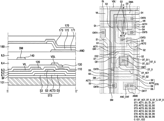
1. A display device, comprising:
a substrate including a display area and a non-display area;
a plurality of signal lines disposed in the display area and extending in a first direction from the non-display area to the display area;
a connection line extending from a portion of the non-display area to a portion of the display area and being electrically connected to a respective signal line of the plurality of signal lines; and
an initialization voltage line extending in a second direction intersecting the first direction,
wherein the connection line overlaps the initialization voltage line in a thickness direction of the display device;
the display device further comprising:
a plurality of anode electrodes disposed above the connection line,
wherein the connection line includes a horizontal portion extending in the second direction, and
wherein at least one anode electrode of the plurality of anode electrodes does not overlap the horizontal portion of the connection line thickness direction of the display device.
|