| CPC G09G 3/3233 (2013.01) [G09G 3/3266 (2013.01); G09G 3/3275 (2013.01); G09G 2300/0819 (2013.01); G09G 2300/0842 (2013.01); G09G 2300/0861 (2013.01); G09G 2310/08 (2013.01)] | 20 Claims |
|
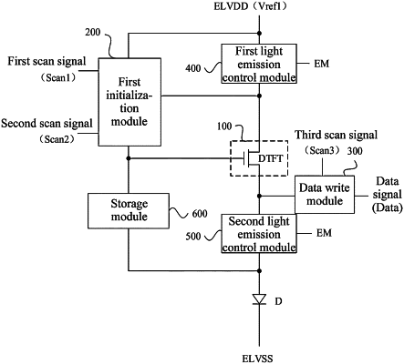
1. A pixel circuit, comprising:
a drive module further comprising a drive transistor, configured to generate, in response to a data signal, a drive current to drive a light-emitting element to emit light;
a first initialization module further comprising a first transistor and a second transistor, controlled by a first scan signal and a second scan signal and is configured to initialize a control terminal of the drive module when the first scan signal and the second scan signal are active; and
a data write module further comprising a third transistor, controlled by a third scan signal, wherein the first initialization module is configured to cooperate with the data write module to write the data signal into the control terminal of the drive module when the second scan signal and the third scan signal are active;
wherein the first scan signal, the second scan signal and the third scan signal have a same waveform shape and a same delay time interval, and scan signals of the pixel circuit multiplex scan signals of previous pixel circuits.
|