| CPC G09G 3/3233 (2013.01) [G09G 3/3266 (2013.01); G09G 3/3283 (2013.01); G09G 2310/08 (2013.01); G09G 2320/0626 (2013.01); G09G 2330/023 (2013.01)] | 15 Claims |

|
1. A driving stage circuit, comprising:
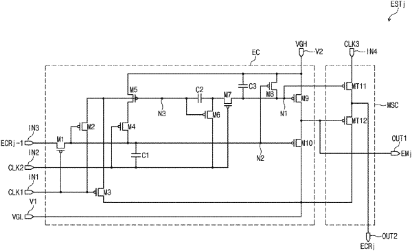
a driving circuit configured to output a driving signal to a first output terminal and output a switching signal to a first node in response to a first clock signal, a second clock signal and a first carry signal; and
a masking circuit configured to receive a masking clock signal different from the first clock signal and the second clock signal and output a second carry signal corresponding to the masking clock signal to a second output terminal in response to, the driving signal, and the switching signal,
wherein the masking clock signal is a signal which is maintained at a first level during a first mode and periodically changes during a second mode.
|