| CPC G09G 3/32 (2013.01) [G09G 2310/0216 (2013.01); G09G 2310/0251 (2013.01); G09G 2310/0267 (2013.01); G09G 2310/067 (2013.01); G09G 2310/08 (2013.01); G09G 2320/0219 (2013.01); G09G 2320/0233 (2013.01)] | 13 Claims |

|
1. A light emitting display device comprising:
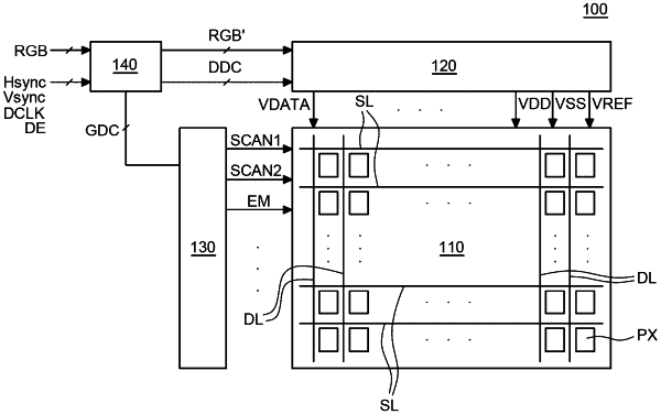
a display panel including a first pixel group including a plurality of pixels in 2N rows, and a second pixel group disposed subsequent to the first pixel group and including a plurality of pixels in 2N rows; and
an emission signal unit including a first emission stage configured to apply the same first emission signal to the first pixel group and a second emission stage to apply the same second emission signal to the second pixel group,
wherein, in a first frame, a falling time of the first emission signal and a rising time of the second emission signal are different from each other,
wherein the falling time of the first emission signal is a time at which the first emission signal is inverted from a high voltage to a low voltage,
wherein the rising time of the second emission signal is a time at which the second emission signal is inverted from the low voltage to the high voltage,
wherein, in the first frame, the falling time of the first emission signal is slower than the rising time of the second emission signal,
wherein, in a second frame, the falling time of the first emission signal is slower than the rising time of the second emission signal,
wherein the falling time of the first emission signal in the first frame and the falling time of the first emission signal in the second frame are different from each other, and
wherein the rising time of the second emission signal in the first frame and the rising time of the second emission signal in the second frame are different from each other.
|