| CPC G09G 3/32 (2013.01) [G09G 2330/021 (2013.01)] | 8 Claims |

|
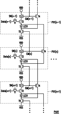
1. A pixel array, comprising:
a plurality of pixels, wherein each of the pixels comprises:
a light emitting diode having an anode and a cathode;
a first transistor having a first terminal that receives a first data signal, a control terminal that receives a first scan signal, and a second terminal;
a second transistor having a first terminal, a control terminal coupled to the second terminal of the first transistor, and a second terminal coupled to the anode of the light emitting diode;
a third transistor having a first terminal that receives a system high voltage, a control terminal that receives a first control signal, and a second terminal coupled to the first terminal of the second transistor;
a fourth transistor having a first terminal coupled to an anode of a light emitting diode of an adjacent pixel, a control terminal coupled to the control terminal of the third transistor, and a second terminal coupled to the cathode of the light emitting diode; and
a fifth transistor having a first terminal coupled to the cathode of the light emitting diode, a control terminal that receives a second control signal, and a second terminal that receives a system low voltage.
|