US 11,886,726 B2
Block family-based error avoidance for memory devices
Michael Sheperek, Longmont, CO (US); Kishore Kumar Muchherla, Fremont, CA (US); Mustafa N. Kaynak, San Diego, CA (US); Vamsi Pavan Rayaprolu, San Jose, CA (US); Bruce A. Liikanen, Berthoud, CO (US); Peter Feeley, Boise, ID (US); Larry J. Koudele, Erie, CO (US); Shane Nowell, Boise, ID (US); and Steven Michael Kientz, Westminster, CO (US)
Assigned to Micron Technology, Inc., Boise, ID (US)
Filed by Micron Technology, Inc., Boise, ID (US)
Filed on Dec. 6, 2021, as Appl. No. 17/542,943.
Application 17/542,943 is a continuation of application No. 16/800,221, filed on Feb. 25, 2020, granted, now 11,231,863.
Claims priority of provisional application 62/950,341, filed on Dec. 19, 2019.
Prior Publication US 2022/0091741 A1, Mar. 24, 2022
This patent is subject to a terminal disclaimer.
Int. Cl. G06F 12/00 (2006.01); G06F 3/06 (2006.01); G06F 12/10 (2016.01); G11C 16/26 (2006.01); G11C 16/04 (2006.01)
CPC G06F 3/064 (2013.01) [G06F 3/0604 (2013.01); G06F 3/0659 (2013.01); G06F 3/0673 (2013.01); G06F 12/10 (2013.01); G11C 16/26 (2013.01); G06F 2212/1041 (2013.01); G11C 16/0483 (2013.01)] 20 Claims
OG exemplary drawing
 
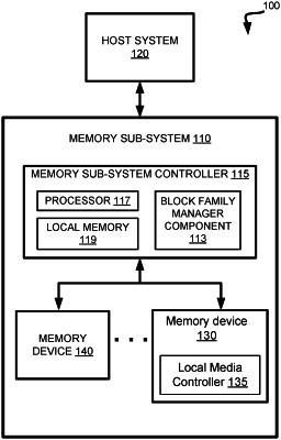
11. A method, comprising:
identifying, by a processing device, based on block family metadata associated with a memory device, a block family associated with a physical block of the memory device;
identifying a first threshold voltage offset bin associated with the block family;
associating the block family with a second threshold voltage offset bin by calibrating an oldest block family associated with the first threshold voltage offset bin;
reading, using a threshold voltage offset associated with the second threshold voltage offset bin, data from the physical block.