| CPC G06F 13/1668 (2013.01) [G06F 1/08 (2013.01); G06F 12/0223 (2013.01); G06F 1/12 (2013.01); G06F 2212/1024 (2013.01); G11C 11/401 (2013.01); H01L 25/0657 (2013.01); H01L 2225/06541 (2013.01)] | 19 Claims |

|
1. A memory, comprising:
a control chip; and
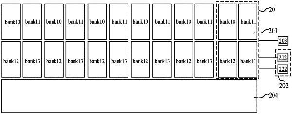
a plurality of storage chips, wherein the plurality of storage chips are electrically connected with the control chip via a common communication channel, the plurality of storage chips comprise a first storage chip set and a second storage chip set, the storage chips in the first storage chip set are configured to perform information interaction with the control chip by adopting a first clock signal, the storage chips in the second storage chip set are configured to perform information interaction with the control chip by adopting a second clock signal, and phase of the first clock signal is different from phase of the second clock signal;
wherein each storage chip comprises at least one channel; the channel comprises: a plurality of storage banks, wherein each storage bank comprises a plurality of storage units, the plurality of storage banks are configured to perform read operation alternately and the plurality of storage banks are configured to perform write operation alternately, a command port, wherein the command port is configured to receive a command signal at a corresponding clock edge, and the command signal is configured to control the read-write operation of the storage banks; and a data port, wherein the data port is configured to receive a data signal to be written into the storage banks or send a data signal at the corresponding clock edge; the corresponding clock edge comprises a clock edge of the first clock signal or a clock edge of the second clock signal; and the command port comprises a row address port and a column address port, the row address port is configured to receive a row address signal of a position where a target storage unit is located, the column address port is configured to receive a column address signal of the position where the target storage unit is located, and the target storage unit is a storage unit selected from the plurality of storage units.
|