| CPC G06F 1/3287 (2013.01) [G06F 1/04 (2013.01); G06F 1/3243 (2013.01); G06F 1/3296 (2013.01)] | 5 Claims |

|
1. A semiconductor device comprising:
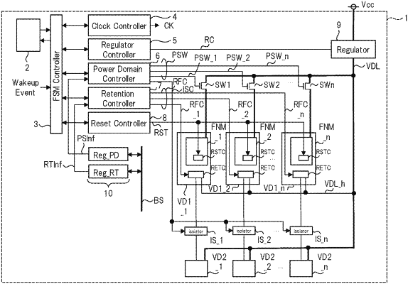
a plurality of first power supply regions in each of which a functional module having a predetermined function is arranged and to which a power supply voltage is individually supplied;
a setting register configured to specify an order of supplying the power supply voltage in the plurality of first power supply regions; and
a power controller configured to supply the power supply voltage to the plurality of first power supply regions in accordance with the order specified by the setting register,
wherein, in a standby state in which the power supply voltage is not supplied to the plurality of first power supply regions, the power controller supplies the power supply voltage to the plurality of first power supply regions in response to an occurrence of a wakeup event in accordance with the specified order,
wherein each of the plurality of first power supply regions includes a retention circuit to which the power supply voltage is supplied in the standby state to retain a state before transitioning to the standby state,
wherein the setting register is configured to specify an order of operating the retention circuits in the plurality of first power supply regions,
wherein the semiconductor device further comprising a retention controller configured to operate the retention circuits in response to the occurrence of the wakeup event in accordance with the order specified by the setting register,
wherein the semiconductor device further comprises a plurality of first isolators connected between the plurality of first power supply regions and a plurality of second power supply regions different from the plurality of first power supply regions, and
wherein the plurality of first isolators connect the plurality of first power supply regions and the plurality of second power supply regions at the same time in response to the occurrence of the wakeup event.
|