| CPC G06F 1/1652 (2013.01) [G06F 1/1616 (2013.01); G09G 3/3233 (2013.01); H10K 77/111 (2023.02); H10K 85/211 (2023.02)] | 15 Claims |

|
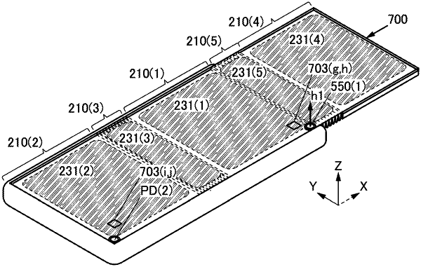
1. A data processing device comprising:
a functional panel;
a first surface;
a second surface;
a third surface;
a fourth surface; and
a fifth surface,
wherein the functional panel comprises a first region, a second region, a third region, a fourth region, and a fifth region,
wherein the second region is configured to perform display in one direction,
wherein the third region is positioned between the first region and the second region,
wherein the third region is configured to be bent,
wherein the fifth region is positioned between the first region and the fourth region,
wherein the fifth region is configured to be bent,
wherein the fourth region is configured to perform display in the one direction in a state where the third region and the fifth region are bent,
wherein the first surface comprises the first region and a light-emitting element,
wherein the light-emitting element emits light,
wherein the second surface comprises the second region and a photoelectric conversion element,
wherein the photoelectric conversion element comprises an organic material, and is formed on a same surface as the light-emitting element,
wherein the photoelectric conversion element is configured to convert the light into an electric signal,
wherein the third surface is positioned between the first surface and the second surface,
wherein the third surface is configured to be bent,
wherein the third surface comprises the third region,
wherein the fourth surface comprises the fourth region,
wherein the fifth surface is positioned between the first surface and the fourth surface,
wherein the fifth surface is configured to be bent,
wherein the fifth surface comprises the fifth region, and
wherein the photoelectric conversion element faces the light-emitting element following the bending of the third surface.
|