| CPC G03F 7/167 (2013.01) [C23C 16/40 (2013.01); C23C 16/45536 (2013.01); C23C 16/45553 (2013.01); C23C 16/50 (2013.01); G03F 7/0043 (2013.01); G03F 7/168 (2013.01); H01L 21/0274 (2013.01)] | 20 Claims |

|
1. A method of forming a photoresist layer over a substrate, comprising:
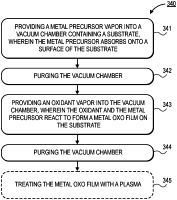
forming a first metal oxo film on the substrate with a first vapor phase process including a first metal precursor vapor and a first oxidant vapor, wherein a flowrate of the first metal precursor vapor and the first oxidant vapor is non-uniform across a surface of the substrate; and
forming a second metal oxo film over the first metal oxo film with a second vapor phase process including a second metal precursor vapor and a second oxidant vapor, wherein a flowrate of the second metal precursor vapor and the second oxidant vapor is non-uniform across the surface of the substrate, and wherein the second oxidant vapor is different than the first oxidant vapor.
|