| CPC G03F 7/0002 (2013.01) [B29C 59/022 (2013.01); C09D 183/14 (2013.01); G03F 7/162 (2013.01); G03F 7/168 (2013.01); B29K 2083/00 (2013.01); B29K 2105/0002 (2013.01)] | 15 Claims |
|
1. A method, comprising:
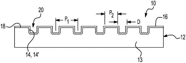
applying a formulation on a surface of a silicon master including a plurality of features positioned at an average pitch of less than about 425 nm, each of the plurality of features having a largest opening dimension being less than about 300 nm, the formulation including:
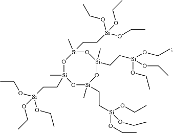
a first silane monomer:
 and
a second silane monomer including a hydrolyzable chloride group, the second silane monomer being present in an amount ranging from 0.001 wt % to less than about 1.4 wt % based on a total weight of silanes present in the formulation; and
curing the applied formulation, thereby forming an anti-stick layer.
|