| CPC G02F 1/13458 (2013.01) [G01R 19/155 (2013.01); G02F 1/133388 (2021.01); G02F 1/133514 (2013.01); G02F 1/134309 (2013.01); G02F 1/136254 (2021.01); G02F 1/133345 (2013.01)] | 17 Claims |

|
1. A liquid crystal display panel, comprising:
a color filter substrate provided with a common electrode layer thereon; and
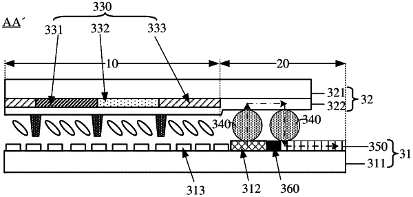
an array substrate arranged in cell alignment with the color filter substrate, and provided with a common electrode line thereon, wherein the array substrate comprises a display area and a peripheral area, the peripheral area comprising a plurality of connection areas; and a plurality of conductive members located on the connection areas and arranged between the color filter substrate and the array substrate;
wherein at least one connection area comprises a conductive sub-region and a detection sub-region, and the conductive members located on the conductive sub-region are respectively in contact with the common electrode line and the common electrode layer, and configured for conducting the common electrode line and the common electrode layer; and
the conductive members located on the detection sub-region are respectively in contact with the common electrode layer and a detection pad, configured for conducting the common electrode layer and the detection pad; and the detection pad is arranged on the array substrate, and the detection pad is not in contact with the common electrode line.
|