| CPC G02F 1/13394 (2013.01) [G02F 1/1337 (2013.01); G02F 1/1347 (2013.01); G02F 1/13439 (2013.01); G02F 1/134327 (2013.01); G02F 1/134336 (2013.01)] | 12 Claims |
|
1. A liquid crystal device comprising:
a first liquid crystal cell; and
a second liquid crystal cell bonded to the first liquid crystal cell, wherein
each of the first liquid crystal cell and the second liquid crystal cell comprises:
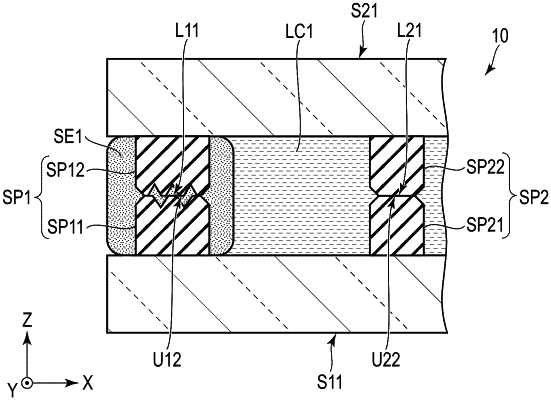
a first substrate comprising a plurality of first electrodes formed in a strip shape;
a second substrate comprising a plurality of second electrodes formed in a strip shape;
a liquid crystal layer held in a gap of 10 μm or more between the first substrate and the second substrate;
a sealant bonding the first substrate and the second substrate together;
one or more first spacers disposed inside the sealant and holding the gap; and
a plurality of second spacers disposed in an effective area surrounded by the sealant and holding the gap,
the first spacer comprises a first lower spacer disposed on the first substrate and a first upper spacer located directly above the first lower spacer and disposed on the second substrate,
each of the second spacer comprises a second lower spacer disposed on the first substrate, and a second upper spacer located directly above the second lower spacer and disposed on the second substrate,
a plurality of the first electrodes comprise a plurality of first strip electrodes configured to have the same voltage applied thereto, and a plurality of second strip electrodes configured to have a voltage different from the voltage applied to the first strip electrodes applied thereto,
the first strip electrodes and the second strip electrodes are alternately arranged,
a plurality of the second electrodes comprise a plurality of third strip electrodes configured to have the same voltage applied thereto, and a plurality of fourth strip electrodes configured to have a voltage different from the voltage applied to the third strip electrodes applied thereto, and
the third strip electrodes and the fourth strip electrodes are alternately arranged.
|