| CPC G02F 1/133707 (2013.01) [G02F 1/133512 (2013.01); G02F 1/134372 (2021.01); G02F 1/136286 (2013.01); G02F 1/133738 (2021.01); G02F 1/133749 (2021.01); G02F 1/133784 (2013.01)] | 4 Claims |
|
1. A liquid crystal display comprising:
a first substrate;
a data line extending in a first direction on the first substrate;
a gate line extending in a second direction on the first substrate;
a first electrode arranged over the data line and the gate line;
an insulating layer on the first electrode;
a second electrode on the insulating layer including:
a connection electrode extending along the data line on the insulating layer,
and a plurality of projection electrodes connected to the connection electrode at one end of each of the projection electrodes, wherein an other end of each of the projection electrodes is separated from the data line in a plan view, and wherein each of the projection electrodes extends in parallel to the gate line in the plan view;
a second substrate facing the first substrate;
a liquid crystal layer between the first substrate and the second substrate;
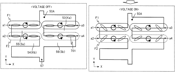
wherein when a predetermined voltage is applied between the first electrode and the second electrode, liquid crystal molecules of the liquid crystal layer in neighboring regions on one side and an other side opposed to each other in a width direction of each of the projection electrodes are rotated in directions opposite to each other to be oriented, and
a black matrix on the second substrate including:
a first black matrix with a constant width in the first direction arranged over the gate line,
and a second black matrix arranged over the data line;
wherein
a width of the first black matrix is wider than a width of the second black matrix,
the second black matrix overlaps the connection electrode so as to dispose the connection electrode inside of the second black matrix in the plan view.
|