| CPC G02F 1/025 (2013.01) [G02B 6/132 (2013.01); G02B 6/136 (2013.01); G02F 1/011 (2013.01); G02F 1/2257 (2013.01); G02F 1/0152 (2021.01)] | 20 Claims |

|
1. A device, comprising:
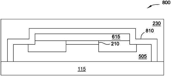
a first waveguide disposed on a substrate, the first waveguide comprising a ridge projecting in a first direction from the substrate and extending in a second direction of an optical path;
a dielectric layer having a lower surface disposed on an upper surface of the ridge; and
a second waveguide comprising a first, planar surface disposed on an upper surface of the dielectric layer opposite the lower surface of the dielectric layer contacting the ridge, wherein a width of the first, planar surface is greater than a width of the dielectric layer and the ridge, and wherein the first waveguide is doped a first conductivity type and the second waveguide is doped a second, different conductivity type; and
a silicon nitride layer disposed on at least three sides of the second waveguide.
|