| CPC G02F 1/025 (2013.01) [G02F 2201/063 (2013.01)] | 28 Claims |
|
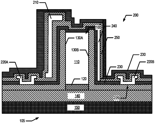
1. A modulator comprising:
a waveguide comprising a waveguide column consisting of a waveguide material, the waveguide column having a first side and an opposite second side, the first and second sides extending out from a substrate;
an etched layer disposed between the waveguide column and the substrate, a first side of the etched layer being in a same plane as the first side of the waveguide column and a second side of the etched layer being in a same plane as the second side of the waveguide column;
a first contact layer (a) disposed on the first side of the waveguide column and the first side of the etched layer and (b) doped with a P-type dopant, wherein the P-type dopant extends from the first contact layer into a first portion of the waveguide column proximate to the first side; and
a second contact layer (a) disposed on the second side of the waveguide column and the second side of the etched layer and (b) doped with an N-type dopant, wherein the N-type dopant extends from the second contact layer into a second portion of the waveguide column proximate to the second side,
wherein the first contact layer and the second contact layer each consist of one or more materials that are different from the waveguide material.
|