| CPC G02B 6/423 (2013.01) [G02B 6/4202 (2013.01); G02B 6/4249 (2013.01); H01L 23/49844 (2013.01); H01L 24/81 (2013.01)] | 21 Claims |
|
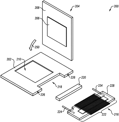
1. An optoelectronic module, comprising:
a stack assembly including an electrical integrated circuit and an optical integrated circuit electrically and mechanically coupled to one another, the optical integrated circuit comprising a first array of electrical couplings positioned around the electrical integrated circuit on a first face of the optical integrated circuit;
an interposer electrically and mechanically coupled to the stack assembly via the first array of electrical couplings and a second array of electrical couplings positioned around a first recess formed in a first face of the interposer;
an adiabatic mode converter positioned in a second recess defined in a side of the interposer, the first recess being separated from the second recess by a portion of the interposer underlying the second array of electrical couplings; and
an optical connector positioned in the second recess and configured to optically couple the optical integrated circuit with an array of optical fibers,
wherein the electrical integrated circuit extends at least partially within the first recess of the interposer.
|