| CPC G02B 6/42 (2013.01) [G02B 6/122 (2013.01); G02B 6/12004 (2013.01); H01L 27/0617 (2013.01); H01L 31/02327 (2013.01); H01L 31/1864 (2013.01); G02B 2006/12061 (2013.01); G02B 2006/12142 (2013.01); G02B 2006/12169 (2013.01); H01L 21/324 (2013.01)] | 8 Claims |
|
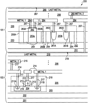
1. A semiconductor structure, comprising:
at least one CMOS structure containing an electronic device formed from a first semiconductor material over a substrate;
at least one photonic device formed from a second semiconductor material disposed above the electronic device, the at least one photonic device having associated microwave activated dopant implants;
a first interlayer dielectric (ILD) metallization structure between the first semiconductor material and the second semiconductor material, configured to electrically couple the electronic device and the at least one photonic device; and
a second ILD metallization structure disposed above the at least one photonic device and electrically coupled to the first ILD metallization structure by a contact passing through the second semiconductor material.
|