| CPC G02B 6/12009 (2013.01) [G02B 6/036 (2013.01); G02B 2006/12061 (2013.01)] | 6 Claims |
|
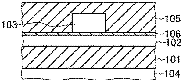
1. An optical waveguide comprising:
a core disposed over a clad layer, wherein the clad layer is disposed over a semiconductor substrate, wherein the core is made of a first semiconductor material, and wherein the core has a rectangular shape in a cross-sectional view;
a spacer layer over the core, wherein the spacer layer comprises an insulator material and directly contacts a top surface of the core, sidewalls of the core, and a top surface of the clad layer; and
a slab layer disposed over and directly contacting the spacer layer, wherein the slab layer is configured to be optically coupled to the core, wherein the slab layer is made of a second semiconductor material, and wherein the first semiconductor material is a compound semiconductor material, and wherein the second semiconductor material is silicon.
|