| CPC G01R 1/07342 (2013.01) [G01R 1/06761 (2013.01)] | 20 Claims |
|
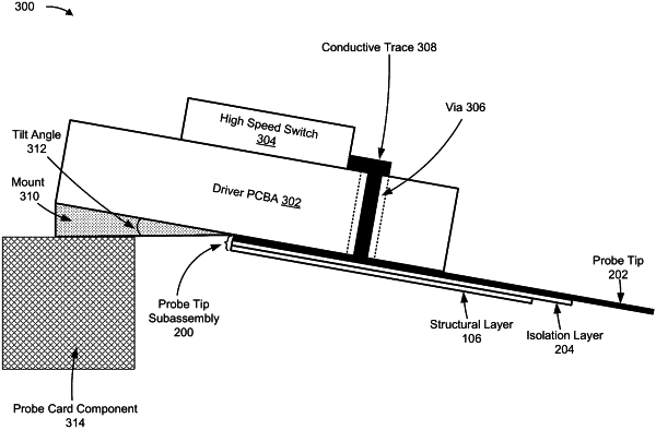
1. A probe tip assembly, comprising:
a driver printed circuit board assembly (PCBA);
a probe tip subassembly comprising:
an isolation layer including a first end and a second end, and
a plurality of probe tips, wherein:
a probe tip, of the plurality of probe tips, includes a first end and a second end,
wherein the first end of the probe tip is aligned with the first end of the isolation layer,
wherein the isolation layer is on only one side of the probe tip, and
wherein the second end of the probe tip extends beyond the second end of the isolation layer; and
a structural layer disposed on only one side of the isolation layer opposite the probe tip,
the isolation layer being disposed between the probe tip and the structural layer;
at least one high speed switch; and
a conductive trace electrically connecting the at least one high speed switch and the probe tip through a via, the via extending from one end at a surface of the driver PCBA through the driver PCBA to another end at the probe tip, and
the PCBA and the probe tip are configured to transmit an electric signal to test an optical component.
|