| CPC G01M 3/047 (2013.01) [G01M 3/16 (2013.01); G01N 25/56 (2013.01); H01L 21/78 (2013.01); H01L 22/26 (2013.01)] | 8 Claims |
|
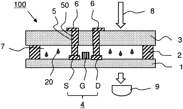
1. A test method of a semiconductor device having a package with an airtight space, which is provided between a substrate wafer in which an element is formed and a cap wafer which is made of a material which can transmit an infrared ray and is provided opposite to the substrate wafer, the test method comprising:
a water applying process in which the semiconductor device is exposed to a moisture atmosphere; and
a leak discrimination process in which an infrared ray transmitted from the semiconductor device is detected and a leak of the package is discriminated based on absorption of the infrared ray by water molecules are included, wherein
the leak discrimination process comprises the steps of:
supplying electric power to the element which is formed in the substrate wafer; and
discriminating the leak of the package based on an infrared ray spectrum, which is radiated from the element and is radiated outside the package.
|