| CPC G01L 1/24 (2013.01) [C09K 11/02 (2013.01); C09K 11/06 (2013.01); C09K 11/574 (2013.01); C09K 11/584 (2013.01); G01N 21/70 (2013.01)] | 14 Claims |

|
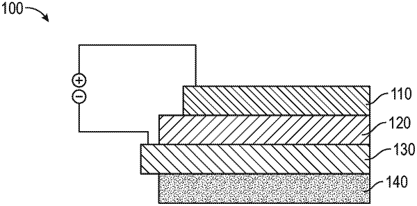
1. A mechanoluminescent device having a vertical device architecture, the device comprising:
an electrode;
a first layer comprising a perovskite;
a counterelectrode;
a substrate;
a second layer comprising a mechanoluminescent material and a matrix material in which the mechanoluminescent material is dispersed;
(i) a first charge transporting layer, (ii) a first charge blocking layer, or (iii) a first charge transporting layer and a first charge blocking layer; and
(a) a second charge transporting layer, (b) a second charge blocking layer, or (c) both a second charge transporting layer and a second charge blocking layer;
wherein the first charge transporting layer, the first charge blocking layer, or both the first charge transporting layer and the first charge blocking layer is arranged between the first layer and the counterelectrode,
wherein the second charge transporting layer, the second charge blocking layer, or both the second charge transporting layer and the second charge blocking layer is arranged between the first layer and the electrode,
wherein the second charge transporting layer is in contact with the electrode,
wherein the first layer is arranged between the electrode and the counterelectrode, and the counterelectrode is arranged between the first layer and the second layer,
wherein the substrate is arranged between the counterelectrode and the second layer, and
wherein the substrate is transparent, flexible, or a combination thereof.
|