| CPC G01J 3/027 (2013.01) [G01J 3/0264 (2013.01); G01J 3/0286 (2013.01); G01J 3/0291 (2013.01); G01J 3/50 (2013.01); G01J 3/52 (2013.01); H01L 23/49838 (2013.01); H01L 25/167 (2013.01)] | 7 Claims |
|
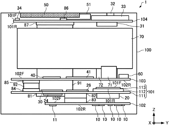
1. An image processing device comprising:
a light receiving element;
a light emitting element;
a battery;
a power source circuit electrically coupled to the battery;
a wireless communication module;
a first substrate provided with the light receiving element;
a second substrate provided with the light emitting element;
a third substrate provided with the power source circuit;
a fourth substrate provided with the wireless communication module; and
a casing storing the first substrate, the second substrate, the third substrate, and the fourth substrate, wherein
the battery is located between the first substrate, the second substrate, and the third substrate, and the fourth substrate.
|