| CPC C23C 16/4404 (2013.01) [C23C 16/308 (2013.01); H01L 21/0228 (2013.01); H01L 21/02126 (2013.01)] | 23 Claims |
|
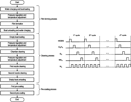
1. A method of processing a substrate comprising:
(a) forming a first film which contains carbon on the substrate by supplying a first processing gas to the substrate in a process container;
(b) forming a second film, which has a material different from a material of the first film, in the process container by supplying a second processing gas into the process container in a state in which the substrate does not exist in the process container; and
(c) forming a third film which contains carbon on the second film formed in the process container by supplying a third processing gas into the process container in the state in which the substrate does not exist in the process container.
|